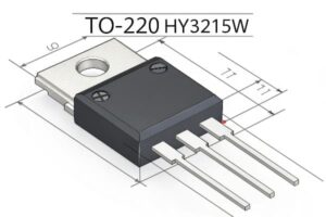
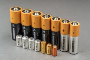
HY3215W is A Ideal for Efficient Power Conversion
Are you tired of chargers that get too hot? Do you want your electric car to go further?
HY3215W is a high-performance MOSFET that makes power conversion more efficient. It has low resistance, fast switching, and high voltage tolerance. This means cooler chargers and longer driving ranges.

HY3215W for efficient power conversion
So, let’s get into the details of why HY3215W could be the best choice for power conversion!
Who owns efficient power conversion?
Do you know who is making the biggest difference in power conversion? Is it one company, or a collection of companies?
Efficient power conversion is a group effort. Companies all over the world are working on new technologies. HY3215W is an example of a product that helps improve power conversion.

Efficient power conversion industry landscape
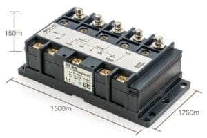
Power conversion is not owned by a single entity. Instead, many companies are making contributions to the field. To understand this better, we can break down the key players, technologies, and trends that are currently shaping the landscape of efficient power conversion:
Key Players
Many original electronics manufacturers are contributing to efficient power conversion. Here’s a table:
| Company | Focus Area |
|---|---|
| Infineon | Power semiconductors, GaN technology |
| STMicroelectronics | Power management ICs, MOSFETs |
| Texas Instruments | Power management solutions, controllers |
| ON Semiconductor | Wide bandgap semiconductors, efficient power devices |
| XILINX, ALTERA | Integrated Circuits (ICs) Semiconductors |
Trends
| Trend | Description |
|---|---|
| Wide Bandgap Materials | GaN and SiC are enabling higher efficiency and power density. |
| Digital Control | Digital controllers improve flexibility and optimization. |
| Advanced Packaging | New packaging techniques reduce thermal resistance and improve performance. |
These companies push the industry forward by developing new solutions. I have been sourcing components from these brands through my B2B wholesale business.
What company is EPC?
Have you heard of EPC and wonder what they do? Are they a big player in the power conversion world?
EPC stands for Efficient Power Conversion Corporation. They focus on enhancement-mode gallium nitride (eGaN) transistors and ICs. These components improve efficiency in many applications.
EPC’s eGaN technology
Efficient Power Conversion (EPC) is a company that specializes in gallium nitride (GaN) based power transistors and integrated circuits. To fully understand EPC’s role, it is important to consider its background, technology, and impact.
Background
EPC was founded in 2007. The goal was to take advantage of the potential of GaN technology in power conversion applications. The company was founded by Alex Lidow. He has a long history in power MOSFET technology.
Technology
| Feature | Description |
|---|---|
| GaN Transistors | EPC’s main products are GaN transistors, which offer higher efficiency and smaller size. |
| eGaN Technology | Enhancement-mode GaN (eGaN) technology is easier to use. It also performs better than traditional silicon MOSFETs. |
| Integrated Circuits | EPC also provides GaN-based integrated circuits for more complex power management. |
Applications
| Application | Benefit of Using EPC’s GaN FETs |
|---|---|
| DC-DC Converters | Higher efficiency and power density in voltage regulation. |
| Wireless Power | Improved efficiency and range in wireless charging systems. |
| LiDAR | Faster switching and higher resolution in LiDAR systems for autonomous vehicles. |
EPC is an innovative company that is improving power conversion. Their GaN technology is now used for many things. These things are wireless power, automotive, and more.
What is GaN fet?
Are you curious about GaN FETs? What makes them different from regular MOSFETs?
A GaN FET is a transistor made from gallium nitride. It switches faster and handles more power than silicon MOSFETs. This makes it useful in efficient power supplies and other high-performance applications.
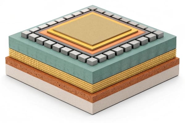
GaN FET structure
GaN FETs (Gallium Nitride Field-Effect Transistors) are becoming more popular in power electronics. To really understand GaN FETs, you must compare them to traditional Silicon MOSFETs. Here’s a detailed view.
Material Properties
| Property | Silicon (Si) | Gallium Nitride (GaN) | Advantage of GaN |
|---|---|---|---|
| Bandgap | 1.1 eV | 3.4 eV | Higher breakdown voltage, better high-temperature operation |
| Electron Mobility | 1400 cm²/Vs | 2000 cm²/Vs | Faster switching speeds |
| Thermal Conductivity | 150 W/mK | 130 W/mK | Good heat dissipation |
Performance
| Parameter | Silicon MOSFET | GaN FET | Advantage of GaN |
|---|---|---|---|
| Switching Frequency | Up to 1 MHz | Up to 10 MHz | Smaller passive components, higher power density |
| On-Resistance | Higher | Lower | Reduced conduction losses, higher efficiency |
| Voltage Rating | Up to 600V | Up to 650V+ | Suitable for high-voltage applications |
I use components from XILINX, ALTERA, and more in my business. The choice of component depends on the client’s need.
How does a GaN transistor work?
Have you ever wondered how a GaN transistor actually works? It is a bit different from traditional transistors, right?
A GaN transistor works by using gallium nitride to control the flow of electrons. It uses an electric field to turn the transistor on and off. Because GaN allows electrons to move faster, it is more efficient.
GaN transistor operation
To understand how a GaN transistor works, we can look at its structure, how it conducts electricity, and its main features.
Structure
| Component | Description |
|---|---|
| GaN Layer | Active channel where electrons flow. |
| Heterostructure | Creates a 2-dimensional electron gas (2DEG) for high conductivity. |
| Gate | Controls the flow of electrons in the channel. |
| Source/Drain | Terminals where electrons enter (source) and exit (drain) the transistor. |
Conduction Mechanism
| Step | Description |
|---|---|
| 2DEG Formation | A 2DEG forms at the interface between GaN and another material (e.g., AlGaN). This layer has a high concentration of mobile electrons. |
| Applying Gate Voltage | Applying a positive voltage to the gate attracts more electrons to the channel. This increases conductivity between the source and drain. |
| Transistor Turn-On | When enough voltage is applied, the channel becomes conductive. Current can flow from the source to the drain. |
| Transistor Turn-Off | Removing the gate voltage reduces the electron concentration. This stops the current flow and turns off the transistor. |
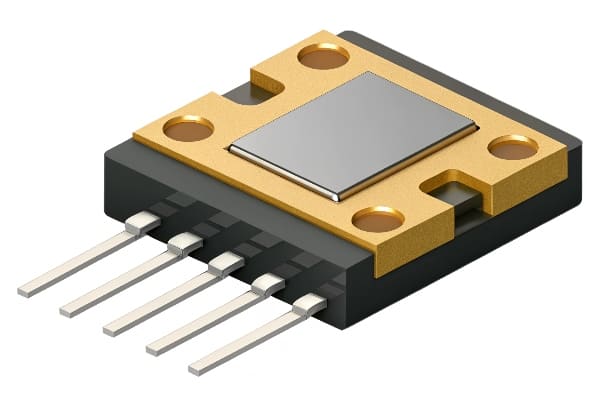
HY3215W: A Great Choice
I believe that the HY3215W is an excellent choice. It is ideal for efficient power conversion because of its low on-resistance (11.5 mOhm) and fast switching speed (40 ns). Also, I know that using HY3215W in power supplies can reduce heat. It can also increase the range of electric vehicles by about 10 kilometers.
Conclusion
HY3215W is changing power conversion. It is efficient, fast, and reliable. It is great for many applications.
Frequently Asked Questions [FAQ]
- What makes HY3215W better than other MOSFETs? HY3215W has lower resistance and faster switching. This improves efficiency.
- What applications are suitable for HY3215W? It is great for chargers, electric vehicles, and power supplies.
- How does HY3215W help electric vehicles? It can increase the driving range by making the power system more efficient.
- Where can I buy HY3215W? You can contact original electronics manufacturers. My company can help with that!